



Intel is moving ahead with production plans around its 18A process technology, but the more interesting story may be the next step: 18A-P. The enhanced node is being positioned as a more polished version of Intel’s 1.8nm-class manufacturing platform, with claimed gains in performance, power efficiency, variability control, and thermal behavior.
That matters for two different reasons. Internally, Intel needs a stronger manufacturing platform for its own client and data center processors. Externally, Intel Foundry needs a node that looks credible to large fabless chip designers weighing alternatives to TSMC and Samsung.
Intel’s pitch for 18A-P is straightforward: keep enough design compatibility with 18A to make migration realistic, while improving the process in ways that matter for actual chips rather than just slide-deck density metrics. The company points to new RibbonFET transistor options, tighter process behavior, better thermal conductivity, and voltage improvements as the main pieces of the update.
The headline figures are notable, but they should still be read as company-provided claims rather than independently proven product results. Intel says 18A-P can deliver up to 9% more performance at the same power, or up to 18% lower power at the same performance and design complexity, compared with baseline 18A. Those numbers came from Intel’s own process disclosures and should not be treated as a guarantee for every finished chip.
18A-P Is More Than a Simple Optical Shrink
The core appeal of 18A-P is that it is not being described as a clean-sheet node. Intel says the process keeps key physical characteristics from 18A, including a 50nm contacted poly pitch and familiar library heights of 180nm and 160nm. In practical terms, that means a design started on 18A may be portable to 18A-P with less disruption than a move to an entirely different node.
That compatibility is important for customers. Chip developers do not choose a process node only because it has a better headline number. They also care about design effort, risk, tool maturity, IP availability, timing closure, packaging options, and how predictable the migration path looks. A node that improves performance and power while preserving some layout and design assumptions can be easier to justify than one that requires a much heavier rework.
Intel’s process update centers on new gate-all-around RibbonFET transistor choices. The company describes high-performance devices with enhanced contacts and new low-power devices. The goal is to give chip designers more options inside the same design: faster devices for timing-critical paths, lower-leakage options for less demanding logic, and a more flexible mix across the chip.
That sort of transistor menu matters because modern processors are not uniform blocks of logic running at one perfect operating point. A CPU, GPU, accelerator, or SoC may include cores, cache, interconnect, media blocks, control logic, SRAM, I/O-adjacent circuitry, and power-management regions that all have different frequency and leakage needs. A process that gives designers more usable device choices can help them tune for the parts of the design that actually constrain performance or battery life.
The larger point is that 18A-P appears to be aimed less at dramatic density scaling and more at practical process maturity. That is not a bad thing. For advanced nodes, incremental gains in variability, voltage behavior, and thermal management can be as important as raw transistor density, especially once designs become power-limited or thermally constrained.
The Performance and Power Claims Need Context
Intel’s most attention-grabbing claim is the 9% iso-power performance gain over 18A. In plain terms, that means a design could run faster at the same power level, at least under the conditions Intel used for its comparison. The alternate claim, an 18% power reduction at the same performance and complexity, points in the other direction: a chip could potentially hit the same target while consuming less energy.
Those are useful numbers, but they are not universal promises. Process-node claims are typically based on specific test structures, reference blocks, standard-cell libraries, or controlled design assumptions. Finished commercial chips can land differently depending on architecture, physical design quality, SRAM behavior, packaging, voltage targets, frequency range, and yield strategy.
For buyers and system builders, the distinction matters. A faster process does not automatically mean every future chip on that node will be 9% faster. A more efficient process does not guarantee every laptop, server, or desktop CPU will see an 18% power drop. It gives designers a better set of tradeoffs, but product-level results depend on how those tradeoffs are used.
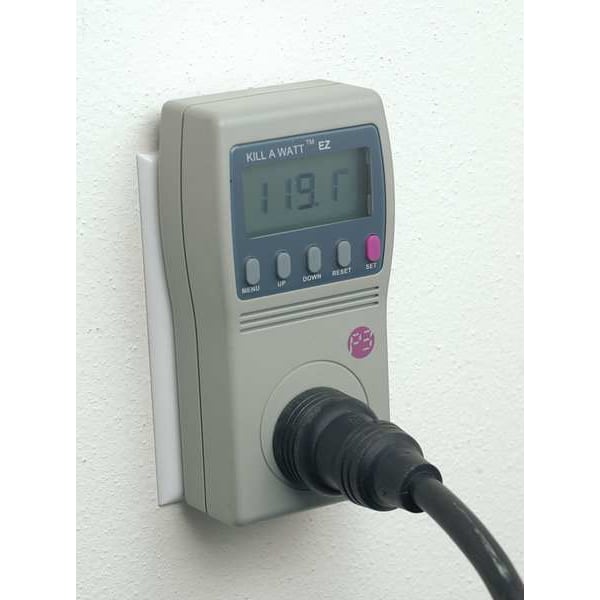
P3 Kill A Watt Electricity Usage Monitor
A plug-in electricity monitor can help readers separate chip-level efficiency claims from the power used by a full desktop or workstation setup. It is most useful for checking wall-power behavior during idle, light-load, and sustained workloads.
Intel also says 18A-P can benefit designs ported from 18A, but the full gains likely require design re-optimization. That is the practical catch. A straightforward port may pick up some process-level improvements, but a chip designed specifically to exploit the new transistor options and voltage behavior should have more room to improve.
That creates a split between short-term and long-term usefulness. For a company already working on 18A, 18A-P could offer a relatively low-friction improvement path. For a new customer, it may be more attractive as a target node from the start, assuming the design ecosystem, IP, capacity, and commercial terms line up.
Variability and Yield Are the Bigger Foundry Questions
Intel also highlights tighter process behavior. One of the more important claims is a 30% tightening of skew corners compared with 18A. In chip design, corner behavior describes how silicon may vary across fast, typical, and slow conditions. Narrowing that spread can make timing and power behavior easier to manage.
A tighter process window can help designers avoid building in as much guardband. It can also improve the odds that more dies land closer to the desired performance and voltage range. Intel presents this as a benefit for parametric yield, meaning the share of chips that meet target electrical specifications, rather than only the share that are defect-free.
That distinction is important. Defect density and parametric behavior are related to manufacturing success, but they are not the same thing. A die can be physically functional yet miss a high-end frequency, voltage, or leakage target. Improvements in variability can help more chips qualify for better bins, but they do not automatically solve every manufacturing-yield challenge.
Intel says 18A-P adds more threshold-voltage options than 18A, moving beyond the earlier set of logic VT pairs. More VT choices can give designers finer control over speed and leakage. In a modern chip, that can matter for both high-performance blocks and low-power regions that spend much of their time idle or lightly loaded.
Still, these claims should be read carefully. Intel is describing the process characteristics it intends to offer, not publishing full production yield data for commercial 18A-P products. Public foundry claims rarely provide the full picture that a large customer would see under NDA, including wafer starts, defect trends, design-rule maturity, SRAM yield, packaging interaction, and long-term reliability data.
That is why 18A-P’s real test will not be whether its paper specifications look better than 18A. They do. The real test will be whether Intel can deliver predictable silicon at volume, with competitive economics, for both its own product groups and outside customers.
For related context, see Intel is moving ahead.
Thermals Could Matter More Than the Headline Speed Gain
Intel says 18A-P improves thermal conductivity by 50%. That is one of the more interesting parts of the disclosure because advanced logic is increasingly limited by heat density, not only by transistor switching speed.
Gate-all-around transistor structures can improve electrostatic control, but advanced nodes also pack high-performance circuitry into extremely dense areas. When a chip pushes more current through dense logic, heat removal becomes a central design constraint. Lower thermal resistance can help maintain performance under sustained load, reduce hotspots, or give designers more flexibility in voltage and frequency planning.
Again, the final product impact will vary. A mobile SoC, a desktop CPU, and a data center processor all use thermal headroom differently. A laptop chip may turn better thermal behavior into quieter operation or longer boost duration. A server processor may use it to support sustained throughput under strict reliability requirements. A small client chip may benefit differently from a large accelerator or multi-chip package.
Intel also points to improved logic negative-bias temperature instability behavior, commonly shortened to NBTI. In practical terms, NBTI is tied to long-term transistor aging under electrical stress. Improvements here are especially relevant for chips expected to operate for years under demanding voltage and temperature conditions.
The company also says 18A-P improves the alignment between logic and SRAM minimum operating voltage. That matters because SRAM arrays often constrain how low a chip can drop its voltage while remaining stable. If logic and SRAM voltage behavior are better matched, designers may have more room to optimize low-voltage operation.
For buyers, this is the kind of process detail that can matter more than it sounds. Better low-voltage stability can affect idle power, light-load efficiency, and battery behavior. Better long-term reliability can matter for servers. Better thermal conductivity can affect sustained performance. None of these features is as easy to market as a single performance percentage, but they can shape the quality of finished silicon.
Why External Customers Will Watch 18A-P Closely
The commercial angle is hard to ignore. Intel is trying to prove that Intel Foundry can serve major external customers, not just Intel’s internal CPU roadmap. 18A is already strategically important, but 18A-P may be the more attractive version for outside companies if it arrives with better maturity, more stable behavior, and a clearer performance-per-watt story.
There have been rumors that large fabless chip designers, including Apple, have evaluated or considered Intel’s advanced nodes. Those reports should be treated as unconfirmed unless the companies announce actual products or manufacturing agreements. Still, the logic behind the interest is easy to understand. The leading-edge foundry market is concentrated, and any credible second source for advanced manufacturing gets attention.
For a company like Apple, Qualcomm, Nvidia, AMD, Broadcom, or another high-volume chip designer, the decision would not be based on one process metric. It would depend on the entire platform: density, power, performance, SRAM, analog and I/O support, packaging, EDA flows, IP, yield learning, capacity, pricing, and the confidence that schedules will hold.
Intel’s challenge is that the foundry business is not just a technology contest. It is also a trust business. Customers need confidence that the node will be ready when promised, that capacity will be available, that design support will be strong, and that Intel will not prioritize its own products in a way that creates risk for external customers.
That is where 18A-P could help, at least on paper. A refined node with better variability and thermals is easier to sell than a first-wave process that still has visible ramp uncertainty. If Intel can show real silicon, competitive yields, and stable schedules, 18A-P could become a stronger foundry offering than baseline 18A.

Semiconductor Manufacturing Technology
Readers who want more background on wafer fabrication, process steps, and manufacturing tradeoffs may find a semiconductor manufacturing textbook more useful than a general business book about chips.
18A-P Also Sits Against a Fast-Moving TSMC Roadmap
Intel is not making these claims in a vacuum. TSMC continues to push advanced logic nodes and packaging roadmaps, and the most demanding AI and HPC customers are increasingly looking beyond transistor density alone. Advanced packaging, chiplet integration, and high-bandwidth memory capacity are now central to the performance roadmap.
TSMC has been outlining larger CoWoS packages with more HBM stacks and more compute silicon over time. That matters because leading AI accelerators are often limited by memory bandwidth, package size, power delivery, and cooling as much as by the logic node itself. A process node that looks good in isolation still has to compete against a broader manufacturing platform.
Intel has its own packaging technologies, including advanced chiplet and 3D integration work, but customer perception will depend on execution. For external foundry customers, a competitive transistor platform is only one part of the offer. The packaging roadmap, supply chain, and proven high-volume delivery are part of the same decision.
This is why the 18A-P story should be read as a step in Intel’s larger foundry reset rather than a standalone win. The node appears to improve several practical aspects of 18A, but Intel still has to prove that those improvements translate into products customers can buy, ship, and trust at scale.
For related context, see variability control and thermal behavior.
The Bottom Line
Intel 18A-P looks like a meaningful refinement of 18A rather than a minor branding update. The company is claiming better performance, lower power, tighter process variation, improved thermal conductivity, more transistor options, and better voltage behavior. Those are exactly the kinds of improvements that can matter as a node moves from early ramp to broader commercial use.
The most practical part of the story is design continuity. If 18A-P keeps enough compatibility with 18A while offering better characteristics, it could give Intel and potential foundry customers a more attractive target without forcing a full reset. That is valuable in a market where schedule risk can be just as damaging as a weak benchmark.
At the same time, the important numbers remain Intel’s claims until they show up in shipping products and customer silicon. A 9% performance gain or 18% power reduction is useful context, but the bigger questions are yield, capacity, cost, reliability, and whether outside customers believe Intel can execute like a leading foundry.
For now, 18A-P strengthens Intel’s story. It suggests the company is not simply trying to get 18A out the door, but is already polishing the process for broader use. Whether that turns into major foundry business will depend less on the headline percentages and more on the silicon Intel can deliver over the next several product cycles.