

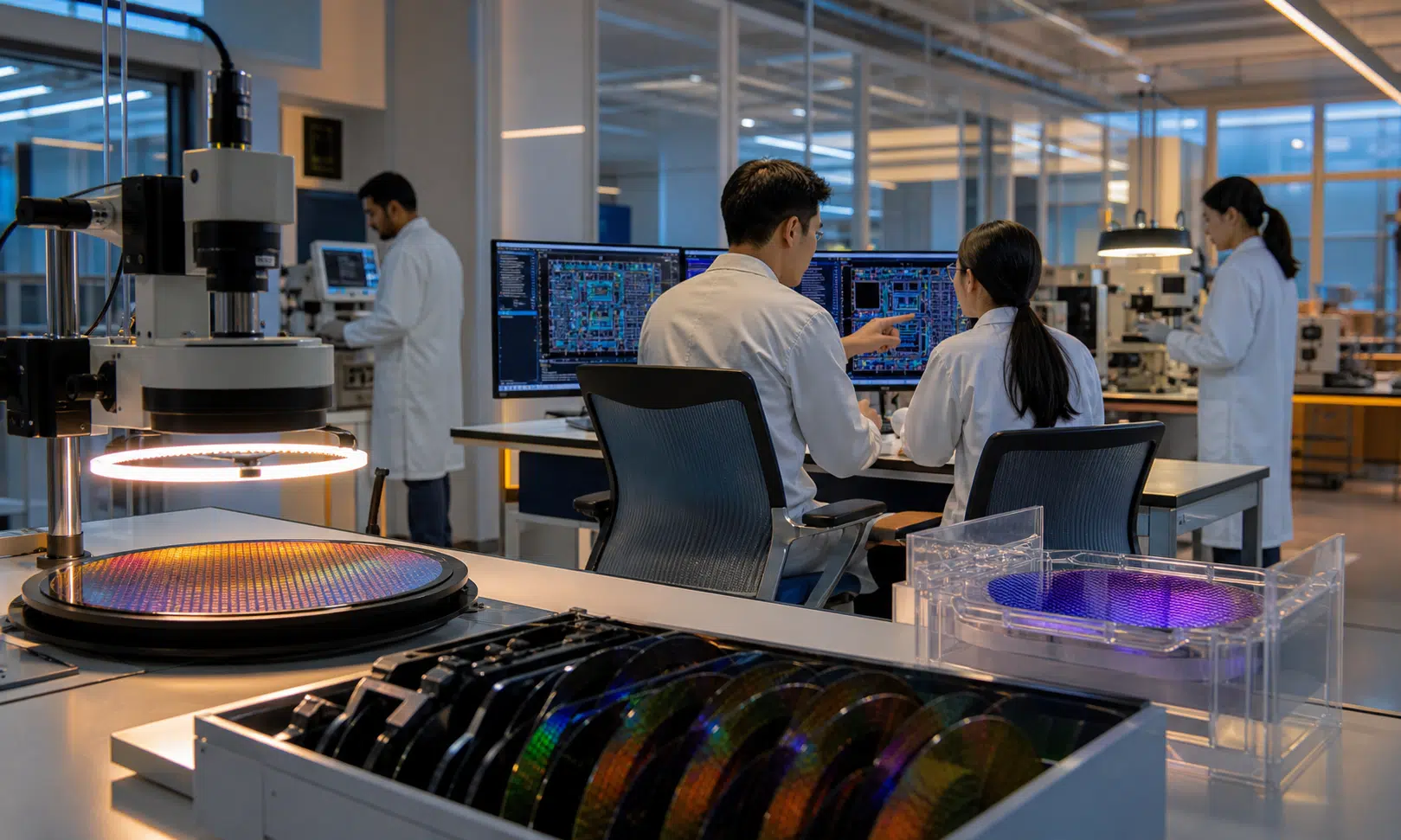

Broadcom, Meta, Applied Materials, GlobalFoundries and Synopsys are teaming with the UCLA Samueli School of Engineering to establish a $125 million Semiconductor Hub focused on AI-era chip research and engineering talent.
The partnership is built around an initial five-year commitment and is meant to connect university researchers more directly with companies working across the semiconductor stack, from design and software to manufacturing, equipment and advanced materials. UCLA said the hub will support research aimed at energy-efficient, AI-powered chip technologies, a priority area as data centers, edge devices and communications systems face rising compute demands.
The effort also gives UCLA faculty and doctoral students a formal path to work with major semiconductor and technology companies on problems that are moving quickly in the commercial market. Ah-Hyung “Alissa” Park, dean of UCLA Samueli, told CNBC that the goal is to shorten the distance between early research and real-world chip innovation.
What the UCLA Semiconductor Hub will focus on
The hub is designed to bring together companies with different roles in the chip ecosystem. Broadcom is a major chip designer and supplier for networking and custom silicon. Applied Materials provides manufacturing equipment and materials engineering expertise. GlobalFoundries is a major contract chipmaker. Synopsys develops chip design software, and Meta has been investing heavily in AI infrastructure and custom silicon.
That mix gives the UCLA program a broad base rather than a narrow research mandate. UCLA said the work will span chip design, equipment, software, manufacturing and related areas of semiconductor development.
The university also described the hub as using a co-design approach, tying together materials, devices and system architectures. That could include work on AI-native hardware and software systems, high-speed data links, energy efficiency, thermal management and advanced packaging.
Internships and workforce development are part of the plan
A major piece of the hub is training. Funding for the program includes yearlong internships with the founding partner companies for UCLA engineering doctoral students.
Park said that industry mentorship, alongside faculty guidance, should give students a clearer and more practical career path. The structure is meant to help Ph.D. researchers understand not only how to work independently in a lab, but also how their work fits into company research pipelines and product timelines.
Applied Materials CEO Gary Dickerson said in a statement that closer ties between industry and academia are increasingly important as semiconductor complexity rises and AI development accelerates. The companies involved are positioning the hub as both a research accelerator and a talent pipeline for U.S. semiconductor work.
Why the timing matters
The launch comes as AI spending reshapes priorities across the technology industry. Companies are pouring capital into data centers, custom accelerators, networking hardware and power-efficient chip designs, even as some large tech firms reduce headcount in other parts of their businesses.
Meta, one of the hub’s founding partners, has been moving through a round of job cuts affecting about 8,000 employees, or roughly 10% of its workforce. That contrast reflects a broader industry shift: companies are cutting costs in some areas while directing more resources toward AI infrastructure and semiconductor capacity.
For UCLA, the hub gives researchers a direct channel into those changes. For the companies, it creates a shared research environment at a university with deep engineering ties to the semiconductor sector. The practical test will be whether the partnership can turn high-risk academic research into usable chip advances quickly enough to matter in a market being pushed hard by AI demand.